Synchronization to Laser Clock
ScanImage® allows the sample clock of the acquisition DAQ to be synchronized to an external clock, most often the laser sync clock. Synchronizing to the laser clock will ensure a constant number of laser pulses per pixel in linear scanning and a consistent relation between laser pulses per pixel as a function of pixel location along a line in resonant scanning (see Resonant Line Formation.)
Tip
Laser pulses per pixel along lines can be calculated using the scanimage utility function Compute Resonant Scan Mask by entering the laser rep rate in place of the DAQ sampling rate.
Synchronization to the laser clock is useful for premium features in ScanImage such as acquisition gating for low rep rate lasers and time correlated photon counting.
The vDAQ has a clock multiplier onboard which is capable of multiplying the external/laser clock so that multiple samples are acquired per laser pulse without the need of extra hardware.
Hardware Configuration
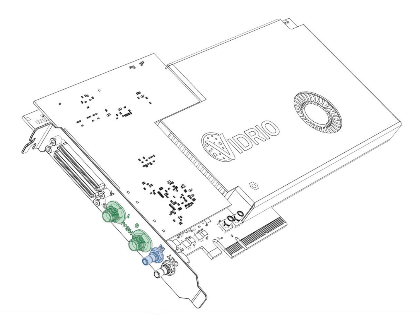
vDAQ Clock Wiring The Laser Clock is connected to the SMB port labeled IN on the vDAQ PCIe card (colored blue). The high speed vDAQ in pictured here. |
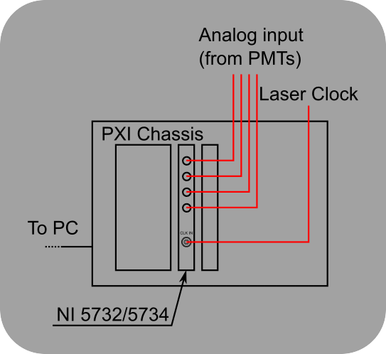
NI Clock Wiring The Laser Clock is connected to the CLK IN SMB connector on the NI FlexRIO adapter module. |
The range of acceptable external clock frequencies is different depending on the DAQ or digitizer used and also on configuration.
If using a vDAQ, the product of the onboard clock multiplier and the external clock frequency must be within the range of acceptable sample rates.
If using NI DAQs, the clock signal provided to the digitizer becomes the sample clock.
An external clock multiplier board such as the AD9516-0 can be used to multiply an incompatible external clock frequency so that it is compatible.
A table is included below with the valid ranges of each of the parameters by DAQ:
DAQ |
External Clock Frequency Range |
Valid Sample rates |
Valid Clock Multipliers |
|---|---|---|---|
vDAQ |
1 MHz - 125 MHz |
62.5 MHz - 125 MHz |
Integers > 0 |
vDAQ-HS with the default bitfile |
62.5 MHz - 84.375 MHz |
2.0 GHz - 2.7 GHz |
32 |
vDAQ-HS with the low rep rate bitfile |
1 MHz - 425 MHz |
2.0 GHz - 2.7 GHz |
Integers > 0 |
NI 5732 |
20 MHz - 80 MHz |
20 MHz - 80 MHz |
Not applicable |
NI 5734 |
50 MHz - 120 MHz |
50 MHz - 120 MHz |
Not applicable |
NI 5771 |
850 MHz - 1.5 GHz |
850 MHz - 1.5 GHz |
Not applicable |
In the case of the high speed vDAQ with the standard bitfile, the external clock must be within the range of 62.5 - 84.375 MHz because the clock multiplier is required to be 32.
Low repetition rate (<62.5MHz down to sub 1MHz) lasers are supported on the high speed vDAQ by configuring a different bitfile. If the external laser clock is below 1 MHz, it can be multiplied via a clock multiplier board to be supported by the hardware. Internally, the vDAQ can be configured to synchronize to the proper rate. For example, a 200 kHz laser clock can be multiplied by 5 to become 1 MHz, which is acceptable by the vDAQ hardware. Internally on the FPGA, it can be configured to divide the 1MHz back to 200 kHz for pixel synchronization.
Note
With the high speed vDAQ using the default bitfile the multiplier must be set to 32. The input range multiplied by 32 gives the range of sampling rates that the vDAQ is capable of - 2.0 GHz to 2.7GHz.
The high speed vDAQ can be configured to use a low rep rate bitfile which allows a wider range of rep rates and the clock multiplier can be set to any value puts the sample rate within the range of 2.0 GHz - 2.7 GHz.
If in doubt of the laser clock signal frequency and amplitude, verify with a high speed oscilloscope set to 50 Ohms input impedance before connecting it to the digitizer.
Tip
The some external clock sources can be difficult to synchronize to for various reasons. The AD9516 clock multiplier board configured with a multiplier of 1 can be used as a buffer to provide a clock which can be used for synchronization
Using the AD-951X Evaluation Board
There are likely other clock multiplying devices that will work, but this is one that we use. Given a clock of dubious wave shape or current driving ability, this clock multiplier board can reliably lock-on and drive the clock input ports of the various ScanImage supported DAQs.
The AD-9516 evaluation board has several versions (AD9516-0, AD9516-1, AD9516-2, etc.). All of the versions are available for sale from Analog Devices on their product page. The AD-9517 and AD-9518 will work as well. We don’t recommend using the AD9516-5 since it doesn’t have a Voltage Controlled Oscillator (VCO). The VCO is used to provide a reliable, jitter free clock signal when one is not available from the laser clock. Without the VCO, you must provide a reliable high speed clock as well as the reference laser clock. The other AD9516-X versions come with a VCO, which we will demonstrate how to synchronize below.
Warning
We don’t recommend using the AD9516-5, it doesn’t have a Voltage Controlled Oscillator (VCO). To use this device, you must have another high-speed jitter free clock source in place of the VCO. The other versions have a VCO.
The software (Rev 2.1.1), which should work for each AD951X board, can be used
to configure the multiplier and the logic output type among other things. If there are further questions, the manual is very helpful.
Go ahead and download and install the software.
Connect the included power adapter and a USB cable, allow drivers to be auto-installed, and launch the software. The software will indicate if the board is recognized/connected at start up:
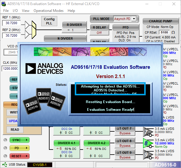
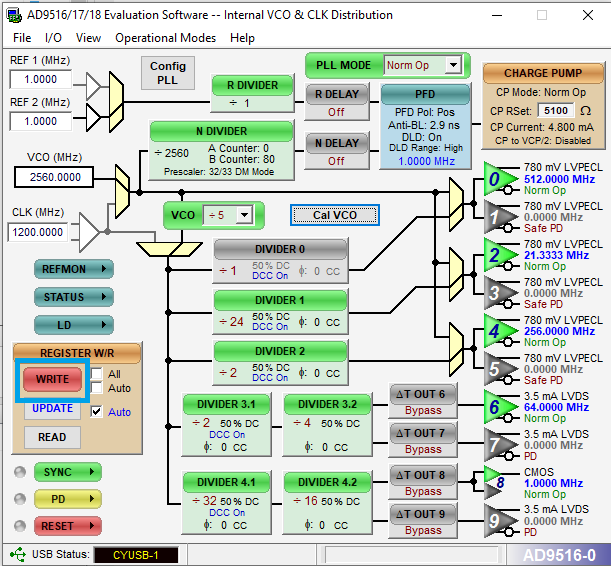
Click in the splash screen to continue. The external clock can be connected to the REF1 or REF2 ports via SMA male - BNC male cable. Here, we will connect the external clock into the REF2 port to increase the output clock frequency.
Note
The AD9516 CLK port is only used when using an external high-speed jitter-free clock. This clock would be used in place of the Voltage Controlled Oscillator (VCO), which is not standard.
The laser clock connects to the REF port in order to generate a cleaner, synchronized clock via dividers from the high frequency clock. The high frequency clock can be from the VCO, or a clock connected to the CLK port. We always recommend using the VCO.
If using a device like the AD9516-5 without a VCO, this port would accomodate a high-speed jitter-free clock in place of the VCO.
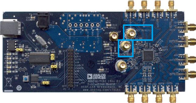
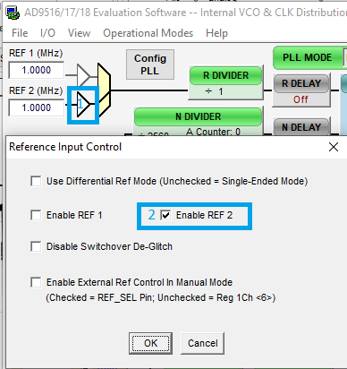
To enable a REF# terminal, left or right click the small white triangle
to reveal a Reference Input Control window. Here, place a check under
the Enable REF 2 checkbox.
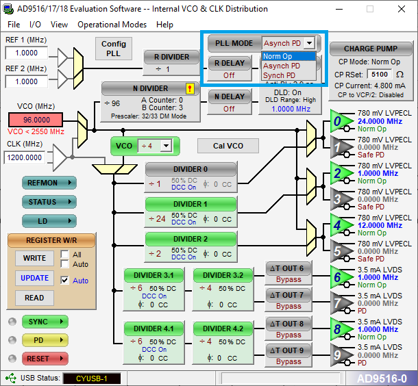
We then synchronize our clock fed into REF 2 to the onboard voltage controlled
oscillator (VCO), using a phase locked loop. For this, we can set PLL Mode to
Normal Op.
From here, we require some configuration settings that vary for different input clock frequencies
and desired output clock frequencies. For this, we have made a
sample MATLAB script which can
calculate each of the parameters. Use this to calculate the A Counter and B Counter
parameters described in the next paragraph. In fact, you can just skip this next
paragraph if you use the MATLAB script. For more info on how to use the function,
see its utility function page.
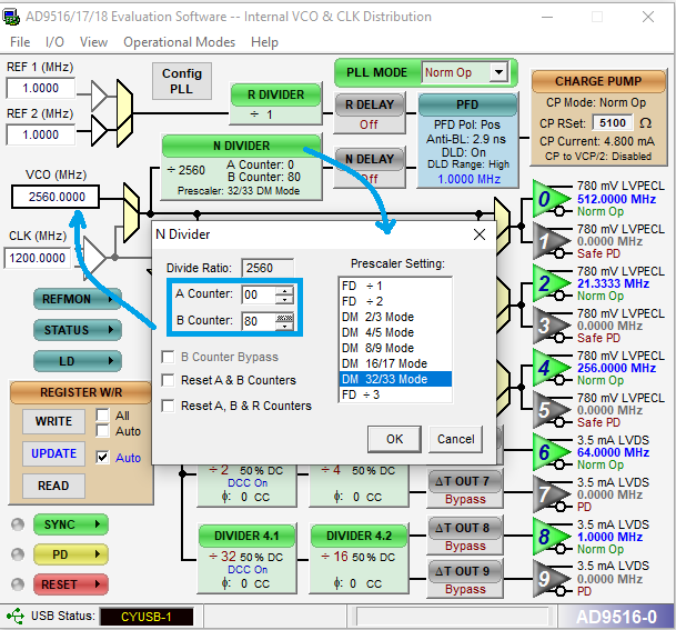
On the AD9516-0, the voltage controlled oscillator (VCO) needs have a frequency of
more than 2550 MHz. To increase it, we need to configure the N Divider. The N Divider’s
Divide Ratio is multiplied by the input clock frequency to calculate the VCO frequency,
and the Divide Ratio is calculated as B Counter * DM Factor + A Counter when the Prescalar Setting is set to DM ##/## Mode. The DM Factor is the numerator of the DM Mode chosen.
E.g., for DM 32/33 Mode, the calculation is 32 * B Counter + A Counter.
For our example of inputting a 1 MHz clock and outputting a 1 MHz clock, let’s have a VCO frequency of 2560 (5 * 32 * 16). For this we need B Counter of 80 and A Counter of 0.
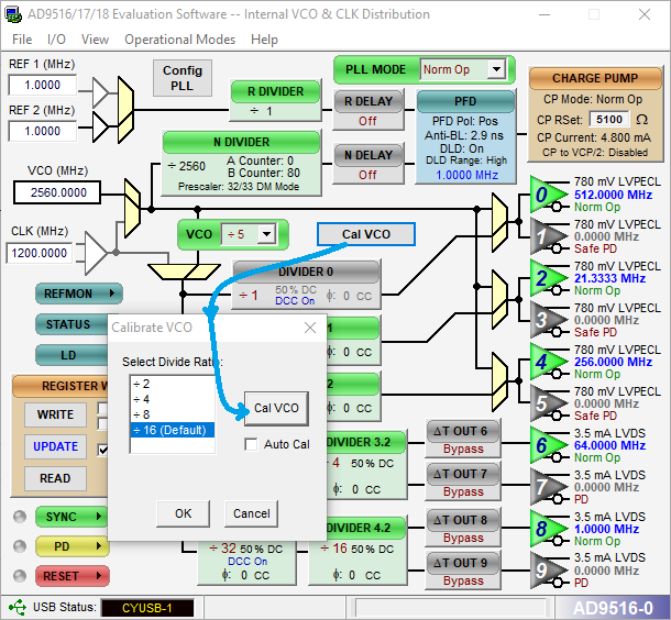
Click OK, and then you need to calibrate the VCO. To do so, click the Cal VCO
button and then click Cal VCO.
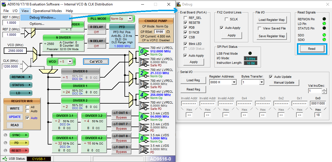
At this point, the PLL should be stable. Verify this by going to View>Debug Window…
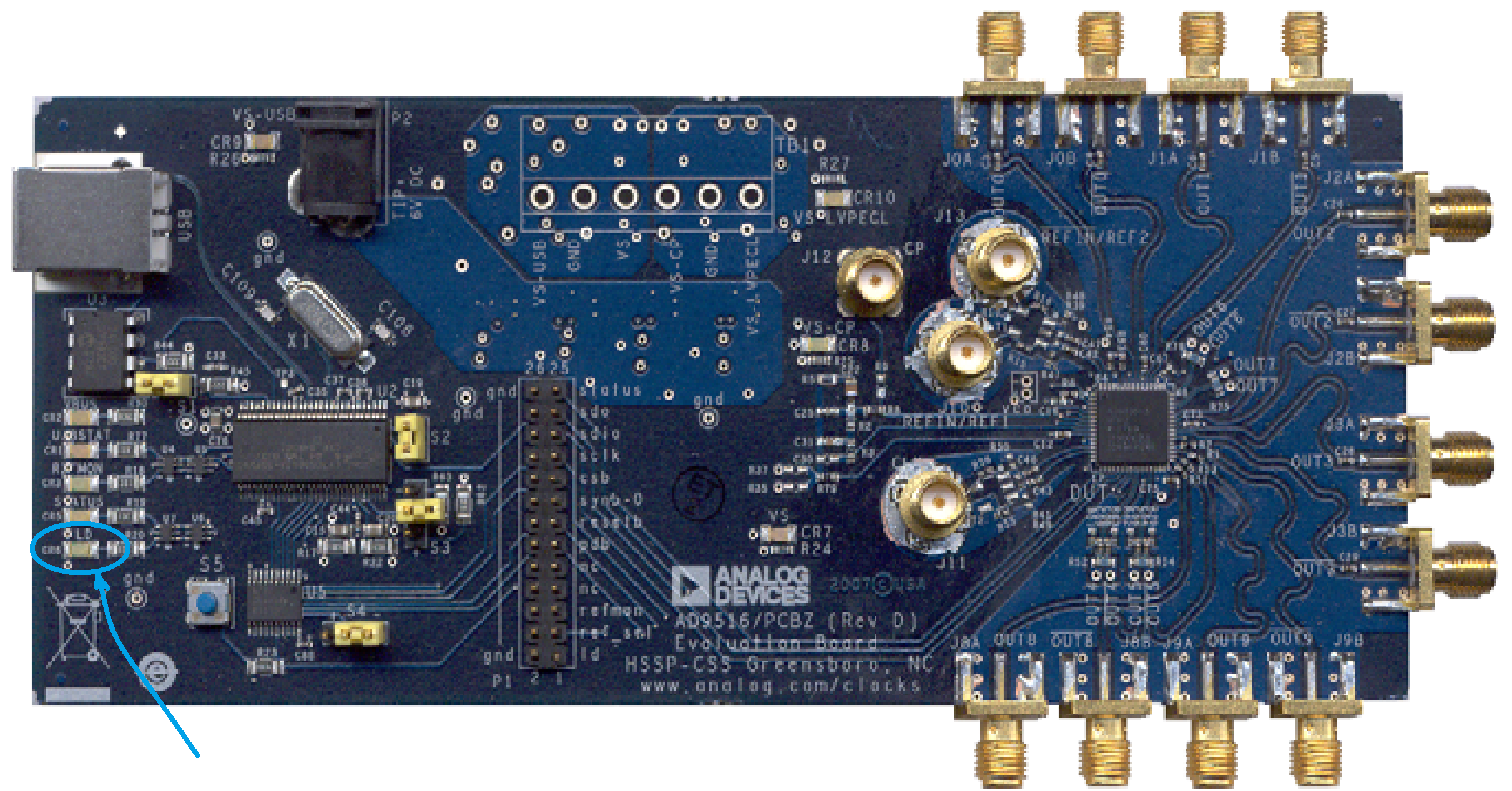
rapidly click the Read button to ensure that the LD Pin light remains on
while reading. You can also just verify that the LD LED on the AD9516 remains on.
|
|
Now, each of the divider values can be entered to divide down the VCO frequency to the output frequency. For this we will input 5 for the VCO clock divider, 32 for first additional divider, and then 16 for the second additional divider in the path towards output.
Note
Each additional divider has a minimum value of 2 (unless bypassed to a value of 1) and a maximum value of 32.
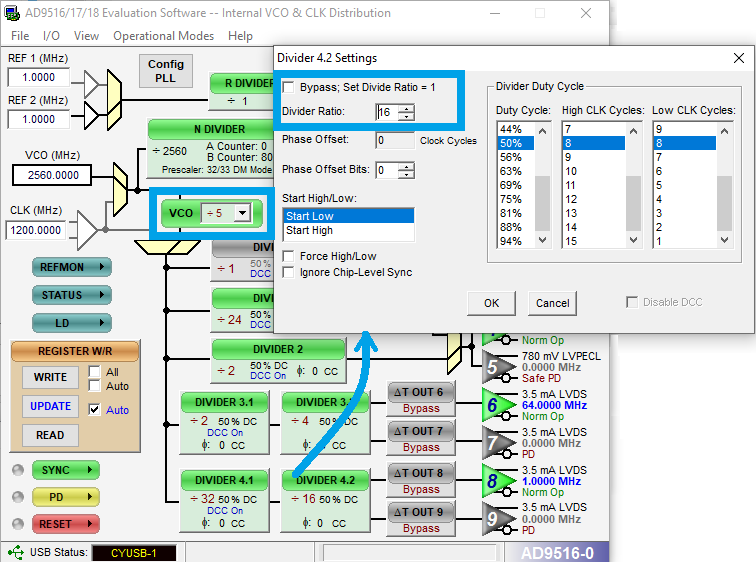
Once the output frequency specified in MHz next to the port gives the intended value,
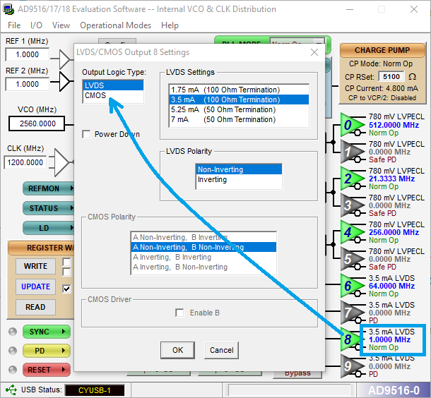
You can specify the output logic type as CMOS.
The last thing to do is to write all this configuration data to the board. Click
the WRITE button inside of the Register W/R panel.
ScanImage® Configuration
Configuration with the vDAQ
There are currently two places where synchronization can be configured for vDAQs:
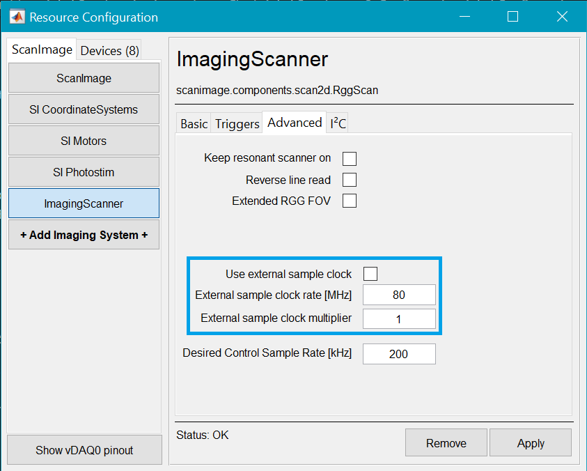
The resource configuration window under the vDAQ Scan System page (scanimage.components.scan2d.RggScan) in the Advanced tab: only available during startup before the user interface is initialized. From the resource configuration, specify whether to sync to an external clock, what the rate of the external clock is, and what to multiply that clock by (i.e. how many samples acquired per rise of the external clock). The product of the laser rep rate and the multiplier must be within the acceptable range of sampling rates of the vDAQ. In the case of the high speed vDAQ with the default bitfile, the multiplier must be set to 32. This will bring the input clock rate from 62.5 - 84.375 MHz to 2.0 - 2.7 GHz. Clicking Apply will apply the sync settings and save them to the machine data file.
The Signal Conditioning Controls window in the auxiliary panel: To configure from the signal conditioning controls, set the clock source to
Externaland select the ClK IN port from the Laser Trigger Settings panel under input terminal. Enter the nominal external clock rate and the multiplier in the Sample Clock Settings panel. Lastly, clickApply Clock Settingsfrom the Sample Clock Settings panel. This will apply the sync settings and save them to the machine data file.
An 80 MHz signal is routed to both the CLK IN and high speed analog input to show synchronization
of sampling to the clock. The synchronization to the
external clock is not achieved until Apply Clock Settings is clicked.
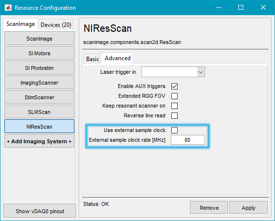
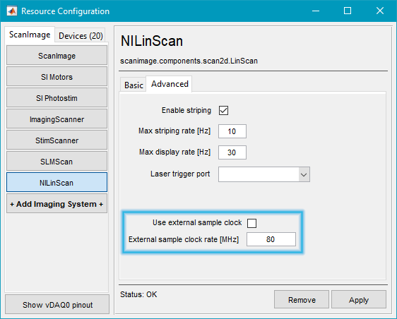
Configuration with NI DAQs
Otherwise, if using NI DAQs, see the advanced tab of the NI Resonant or NI Linear Scan System configuration. There is no onboard clock multiplier, so if multiple samples per laser pulse is desired, then an external clock multiplier such as the AD9516 can be used.
|
|
Note
The laser trigger port is specified separately as it is possible to gate or temporally demux signals without synchronization. It is also possible to gate or temporally demux signals relative to a slower laser when sampling is synchronized to a second, faster laser.
In every case, the parameter External Sample Clock Rate is the nominal rate of the external clock and is used within ScanImage® as a first approximation to determine the scan parameters. To ensure maximum accuracy, ScanImage® will validate the stability and exact rate of the laser clock on every start of an Acquisition. If ScanImage® detects an unstable clock, it will report an error and abort the acquisition.
Troubleshooting
Laser Clock Filtering
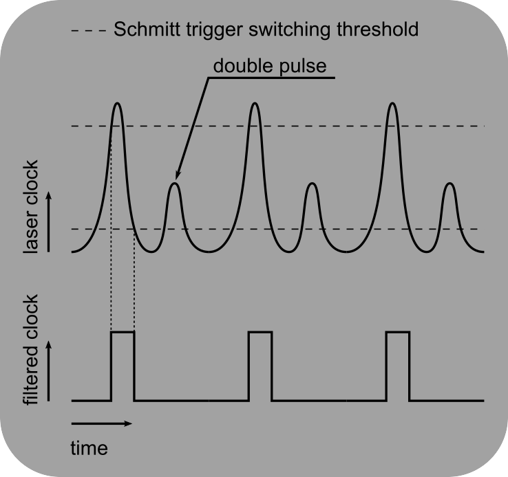
A noisy laser clock can cause the acquisition DAQ to become unstable. An external circuit (e.g. a Schmitt Trigger) is required to clean the clock for use with ScanImage.
Laser Clock Signal Quality
The external clock connected to the NI digitizer module must comply to the parameters outlined in the NI5732/5734 user manual, page 36, section ‘CLK IN’. If the fast photodiode output of the laser (laser clock output) does not fulfill these specifications, the signal needs to be filtered by an external circuit (e.g. a Schmitt trigger) before it can be connected to the digitizer input (See figure at right).
Alternatively, an external fast photodiode can be used that fulfills the electrical specifications required by the NI digitizer module.
Attention For high frequency signals, electrical termination is required. The NI5732/5734 Clock input connector is single-ended with a 50Ohm termination. Use cables with 50Ohms characteristic impedance and make sure the source of the clock signal is 50Ohm terminated as well. Correct impedance matching will eliminate reflections in the transmission line. |
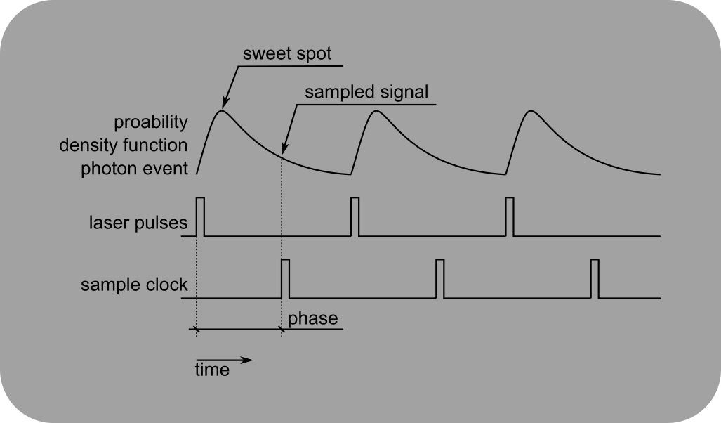
Sampling Phase Delay
Various delays can lead to a phase offset between the sampling sweet spot and the actual sampling of the signal.
Sampling Phase Delay
Delays between the emission of the laser pulse and the registration of a sample clock by the digitizer lead to a phase shift between the laser pulse and the acquisition of the PMT signal. This phase shift depends on delays in the photodiode that generates the laser pulse clock, cable delays and ultimately on delays in the PMT and preamplifier.
With a vDAQ, such phase delay can be accounted for with the Trigger Filter (Ticks) setting within the laser trigger settings panel of the Signal Conditioning Controls window. Ticks is a unit of time defined as the duration between two consecutive samples. At the moment, between successive launches of ScanImage, the trigger filter may need adjustment to realign sampling to the PMT signal.
Alternatively, a delay switch box can be used.
Tip
The laser pulse separation time of a laser with 80MHz repetition rate is 12.5ns. Because of this short time interval a crude way of adjusting the phase is to vary the cable length used for connecting the laser clock output to the FlexRIO digitizer module in a range of c*12.5ns = 3.7m
Anti-Aliasing Filter
By default with the NI 5732/5734, ScanImage® enables a hardware Bessel filter to eliminate aliasing effects and to reduce high frequency interference (see NI 5732/5734 manual page 17,22). When syncing to a laser clock, it might be preferable to deactivate this filter in software. To change the filter settings of the FlexRIO digitizer module, After starting ScanImage, enter the following command in the Matlab command window:
>> hSI.hResScan.channelsFilter = ‘none’;
The property hSI.hResScan.channelsFilter accepts three possible values: ‘none’ ‘bessel’ ‘elliptic’.